(China (Mainland))

Product Summary
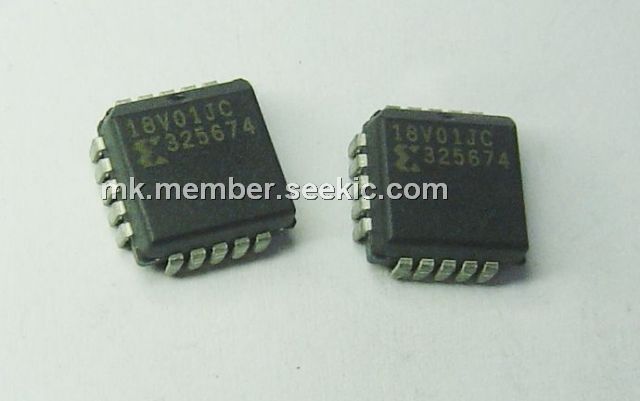
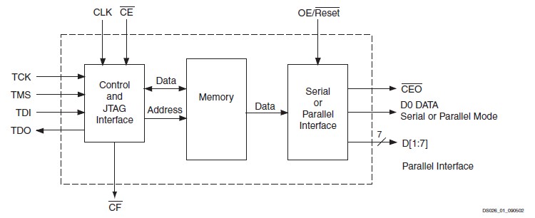
The XC18V01JC is an in-system programmable configuration PROM. It includes a 4-megabit, a 2-megabit, a 1-megabit, and a 512-kilobit PROM that provides an easy-to-use, cost-effective method for re-programming and storing Xilinx FPGA configuration bitstreams. When the FPGA is in Master Serial mode, the XC18V01JC generates a configuration clock that drives the PROM. A short access time after CE and OE are enabled, data is available on the PROM DATA (D0) pin that is connected to the FPGA DIN pin. The XC18V01JC can be concatenated by using the CEO output to drive the CE input of the following device.
Parametrics
XC18V01JC absolute maximum ratings: (1)VCCINT/VCCO Supply voltage relative to GND: –0.5 to +4.0 V; (2)VIN Input voltage with respect to GND: –0.5 to +5.5 V; (3)VTS Voltage applied to High-Z output: –0.5 to +5.5 V; (4)TSTG Storage temperature (ambient): –65 to +150 ℃; (5)TSOL Maximum soldering temperature (10s @ 1/16 in.): +220 ℃; (6)TJ Junction temperature: +125 ℃.
Features
XC18V01JC features: (1)IEEE Std 1149.1 boundary-scan (JTAG) support; (2)Simple interface to the FPGA; (3)Cascadable for storing longer or multiple bitstreams; (4)Low-power advanced CMOS FLASH process; (5)Dual configuration modes: Serial Slow/Fast configuration (up to 33 MHz); Parallel (up to 264 Mb/s at 33 MHz); (6)5V tolerant I/O pins accept 5V, 3.3V and 2.5V signals; (7)3.3V or 2.5V output capability; (8)Available in PC20, SO20, PC44, and VQ44 packages; (9)Design support using the Xilinx Alliance and Foundation series software packages.; (10)JTAG command initiation of standard FPGA configuration.
Diagrams
 |
 XC1800 |
Other |
|
Data Sheet |
Negotiable |
|
||||||
|
XC18V00 |
Other |
|
Data Sheet |
Negotiable |
|
||||||
|
XC18V02 |
Other |
|
Data Sheet |
Negotiable |
|
||||||
|
XC18V02VQG44C |
Other |
|
Data Sheet |
Negotiable |
|
||||||
|
XC18V04VQ44C |
|
IC PROM SRL FOR 4M GATE 44-VQFP |
Data Sheet |
|
|
||||||
|
XC18V04VQG44C |
|
IC PROM REPROGR 4MB 44-VQFP |
Data Sheet |
|
|
||||||